Introduction
Panelizing PCBs is often required when making a smaller PCB than the minimum size a fabrication house accepts. However, it is not straightforward for the hobbyist to do it without expensive software tools.
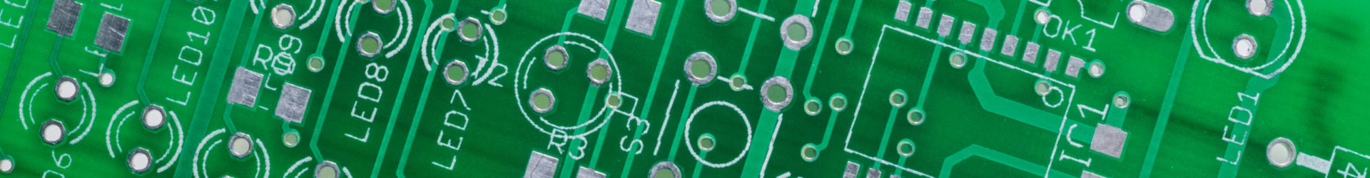
In the below example I am using Eagle 6.3.0 and a small design of mine, the Spindicator Clone.
I use Eagle to design my circuits – the free version is enough for most hobbyists and there is a wealth of information, tutorials on how to use several aspects of it.
The problem
The obvious way to panelize PCBs in Eagle is almost as easy as copying and pasting the whole board. These are the steps I followed:
-
- Open design in Eagle.
- Make sure only the PCB designer is open. Close the schematics design tool if necessary, otherwise the following steps will not work. Depending on the version of Eagle you are using, you may get a warning message at the top of Eagle, which you can safely ignore.

This is expected as if we now make modifications on the PCB they won’t be reflected in the schematics. - Click on the Copy tool.
- Click on the Group tool.
- Draw a selection rectangle in a way that the whole design, including the dimensions of the design, is selected. If you did this correctly, all the parts, texts, etc. are highlighted.
- Press Ctrl+right mouse click to create a copy of the board.
- Move the newly created copy next to the original, then place it there by clicking with the left mouse button.
 |
| I tend to leave a bit of space between each board as a safety margin – you can always file off unwanted extras, but you cannot grow back missing areas later. |
- From now on you can use the Paste tool to add additional copies of the same board.
The problem is noticeable already after the first copy is placed on the board: Once the copy is placed on the board, Eagle automatically changes the part names to avoid duplication. Normally this is not a problem, but when you want to panelize a design you want all the panels to come out exactly the same.
 |
| You can see that LED1 becomes LED11, OK1 becomes OK2, Ic1 becomes IC2 and so on. This is clearly not acceptable. |
Of course, Eagle wouldn’t let me manually revert the part names, but even if it did, it would be quite some work to do it on all the copies, and errors would be hard to avoid.
Solution
I did some research on the internet if this subject has been covered before me, but all I found was either using Photoshop for multiplying the film for photo transfer (not usable for me as I need to send Gerber files to the fab house) or using some specialized 3rd party application to panelize the gerber files directly. This latter one would probably be a way of doing it, but I am a bit paranoid about installing new software on my computer – I only install new software on my work computer if it’s absolutely unavoidable.
Then I remembered that Eagle comes with support for User Language Programs (ULPs) which is, in essence, a way of creating some automation within Eagle. This is Eagle’s own definition of ULP: “The EAGLE User Language can be used to access the EAGLE data structures and to create a wide variety of output files.”
Eagle comes with a number of ULPs preinstalled, ready for you to use. Since I didn’t find any description of these included ULPs I started to have a look at them to see if there is one that would put me in the right direction and maybe with some modifications/additions I could use it for panelizing.
To my surprise I found one that’s called panelize.ulp. Wow, this must be close! Since I have no clue (yet) as to how to use/modify these ULPs I gave it a try anyway to see what it does.
 |
| In the file menu click on Run…, then find this ULP and run it. |
On this tiny board it took like zero seconds to run. The result was like this:
 |
| The yellow part names easily visible. |
It seems to me that all this ULP does is duplicate all the part names (like IC1) on the 125th (tNames) layer:

Now let’s see what happens when I multiply this design:

You can see that the part names are still automatically corrected by Eagle (bad for us) but the original part names (in yellow) are all preserved (yay!).
Now the only thing left is to tell the CAM processor that we want to export the newly created layer(s) rather than the original ones. This is done in the CAM settings page:
- Click on the CAM tool.
- In the File menu select Open -> Job…
- Open the CAM job you usually use to create your gerber files for the fab house.
- Click on the Silk top tab to display which layers will get exported to become the silk screen.
Normally, I have the following layers selected:- 20-Dimension
- 21-tPlace
- 25-tNames
- 121-tSilk
- Remove selection from Layer 25 (tNames) as this contains the original part names
- Select Layer 125 (_tNames) as this contains the new part names
Done! If you now run the CAM processor you will have a set of gerber files that will result in identical PCBs.
Verification
I use gerbv, an open source, cross platform gerber file viewer for the final check before I send PCBs for manufacturing.
 |
| Final panelized board as seen in the Gerber file viewer. |
This view shows only the top silk screen layer:
 |
| Part numbers are consistent throughout the panel. |
This panelized PCB is now ready for manufacturing!
Last word
All this work is based on my experiences and may not be the simplest way to accomplish the goal set. If you think you have a better/faster/more elegant way of getting the same output from the same input files please let me know in the comments.

The bigger problem is how do you make cuts to de-panelize the boards? Short of using a bandsaw, I don't know of a decent way to do this w/o modifying the gerbers to have at least some v cuts…
I usually use a blade to do this. After a few strikes the board breaks relatively easily.
kenkyee: You'd be wanting the Vscore layer, layer 102. This will allow you to specify to the fab where to place Vscore lines. You'll need to include this information in a suitable format for your fab when you CAM job convert your Eagle board to Gerber format.
Thanks for the tip, I'll try this next time.
Hi Viktor, the images have disappeared?
Well, this article is migrated from my old blog and some pics indeed seem to have issues, but in this case I seem to be able to display all of them. Which one do you mean?